Related Page: Grid Driven Amplifiers
Screen supply design is far more critical than we might realize. The screen grid, is far more dominant than the anode in tube operation. The screen current is far more critical to tube life or amplifier function than control grid current.
Small screen voltage variations cause large changes in a tube's zero signal operating point (quiescent current) and power gain. In all transmitters and amplifiers, with the general exception of rules 2-4 below, stages that are not subject to tuning or operated in class A should follow these rules:
2.) screen dissipation must be limited to a value safely below the tube's rated maximum screen dissipation under all conditions
3.) screen voltage should be held at the proper safe voltage range under all normal operating conditions, even key up
4.) as the screen goes into dissipation overload, screen voltage should be immediately reduced or removed
Linear and Non-linear Stages
The screen grid is the main "attracter" of electrons in a normal multi-grid tube. Screen grid voltage has far more influence on tube current than anode voltage. This is why, using only screen regulation, oscillators can be stabilized for supply voltage changes.
For a 6L6, we find open cathode voltage more than doubles as screen voltage doubles. Cathode voltage barely changes with anode voltage changes!
All stages (with the possible exception of some class A stages), linear or not, should regulate or reasonably control screen voltage, but linear stages are especially critical for screen voltage. Even though proper design technique of linear stages dictates a very tightly regulated screen supply, linear amplifiers sometimes cheap out and use non-regulated screen supplies.
It is easy to see why old designs avoided screen regulation. Prior to the 1970's a good screen system was technically difficult, took up a lot of space, and was relatively expensive. Today, all of this can be accomplished in most circuits with a few very and relatively inexpensive components. In all examples below, screen dissipation will not exceed the static regulator dissipation as long as screen supply voltage is at least twice regulated screen voltage. As a matter of fact, at just 1.5 ratio between Vsg (screen operating voltage) and Vss (screen supply voltage), screen dissipation is well-limited.
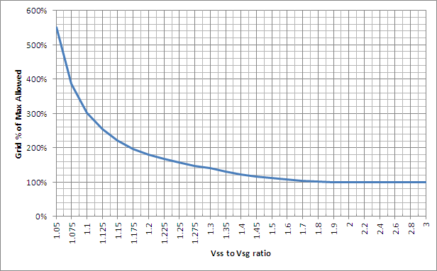
With screen supply voltages much over 2x desired voltage, and with a regulator at the screen grid, excessive fault dissipation in R1 and wasted supply power become disadvantages. This can be a trade off for supply cost:
| Opr V g2 | Norml Disp g2 | Scrn Supply V | allowed Ig2 | maximum Ig2 | Screen Drop Res | Normal Pd R | Fault Pd R | Max Pd g2 | Max PdReg | Pd OL % | Ratio HV/Eg2 |
| 100 | 3 | 105 | 0.0300 | 0.6300 | 167 | 0.15 | 66.15 | 16.54 | 3.00 | 551% | 1.05 |
| 100 | 3 | 107.5 | 0.0300 | 0.4300 | 250 | 0.23 | 46.23 | 11.56 | 3.00 | 385% | 1.075 |
| 100 | 3 | 110 | 0.0300 | 0.3300 | 333 | 0.30 | 36.30 | 9.08 | 3.00 | 303% | 1.1 |
| 100 | 3 | 112.5 | 0.0300 | 0.2700 | 417 | 0.38 | 30.38 | 7.59 | 3.00 | 253% | 1.125 |
| 100 | 3 | 115 | 0.0300 | 0.2300 | 500 | 0.45 | 26.45 | 6.61 | 3.00 | 220% | 1.15 |
| 100 | 3 | 117.5 | 0.0300 | 0.2014 | 583 | 0.53 | 23.67 | 5.92 | 3.00 | 197% | 1.175 |
| 100 | 3 | 120 | 0.0300 | 0.1800 | 667 | 0.60 | 21.60 | 5.40 | 3.00 | 180% | 1.2 |
| 100 | 3 | 122.5 | 0.0300 | 0.1633 | 750 | 0.68 | 20.01 | 5.00 | 3.00 | 167% | 1.225 |
| 100 | 3 | 125 | 0.0300 | 0.1500 | 833 | 0.75 | 18.75 | 4.69 | 3.00 | 156% | 1.25 |
| 100 | 3 | 127.5 | 0.0300 | 0.1391 | 917 | 0.83 | 17.73 | 4.43 | 3.00 | 148% | 1.275 |
| 100 | 3 | 130 | 0.0300 | 0.1300 | 1,000 | 0.90 | 16.90 | 4.23 | 3.00 | 141% | 1.3 |
| 100 | 3 | 135 | 0.0300 | 0.1157 | 1,167 | 1.05 | 15.62 | 3.91 | 3.00 | 130% | 1.35 |
| 100 | 3 | 140 | 0.0300 | 0.1050 | 1,333 | 1.20 | 14.70 | 3.68 | 3.00 | 123% | 1.4 |
| 100 | 3 | 145 | 0.0300 | 0.0967 | 1,500 | 1.35 | 14.02 | 3.50 | 3.00 | 117% | 1.45 |
| 100 | 3 | 150 | 0.0300 | 0.0900 | 1,667 | 1.50 | 13.50 | 3.38 | 3.00 | 113% | 1.5 |
| 100 | 3 | 160 | 0.0300 | 0.0800 | 2,000 | 1.80 | 12.80 | 3.20 | 3.00 | 107% | 1.6 |
| 100 | 3 | 170 | 0.0300 | 0.0729 | 2,333 | 2.10 | 12.39 | 3.10 | 3.00 | 103% | 1.7 |
| 100 | 3 | 180 | 0.0300 | 0.0675 | 2,667 | 2.40 | 12.15 | 3.04 | 3.00 | 101% | 1.8 |
| 100 | 3 | 190 | 0.0300 | 0.0633 | 3,000 | 2.70 | 12.03 | 3.01 | 3.00 | 100% | 1.9 |
| 100 | 3 | 200 | 0.0300 | 0.0600 | 3,333 | 3.00 | 12.00 | 3.00 | 3.00 | 100% | 2 |
| 100 | 3 | 220 | 0.0300 | 0.0550 | 4,000 | 3.60 | 12.10 | 3.00 | 3.00 | 100% | 2.2 |
| 100 | 3 | 240 | 0.0300 | 0.0514 | 4,667 | 4.20 | 12.34 | 3.00 | 3.00 | 100% | 2.4 |
| 100 | 3 | 260 | 0.0300 | 0.0488 | 5,333 | 4.80 | 12.68 | 3.00 | 3.00 | 100% | 2.6 |
| 100 | 3 | 280 | 0.0300 | 0.0467 | 6,000 | 5.40 | 13.07 | 3.00 | 3.00 | 100% | 2.8 |
| 100 | 3 | 300 | 0.0300 | 0.0450 | 6,667 | 6.00 | 13.50 | 3.00 | 3.00 | 100% | 3 |
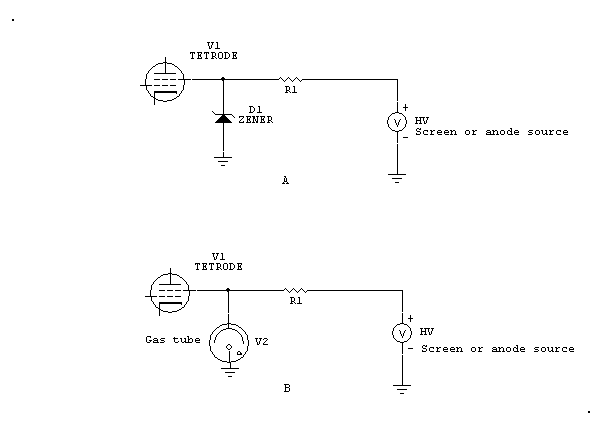
Typical regulated screen circuits are:
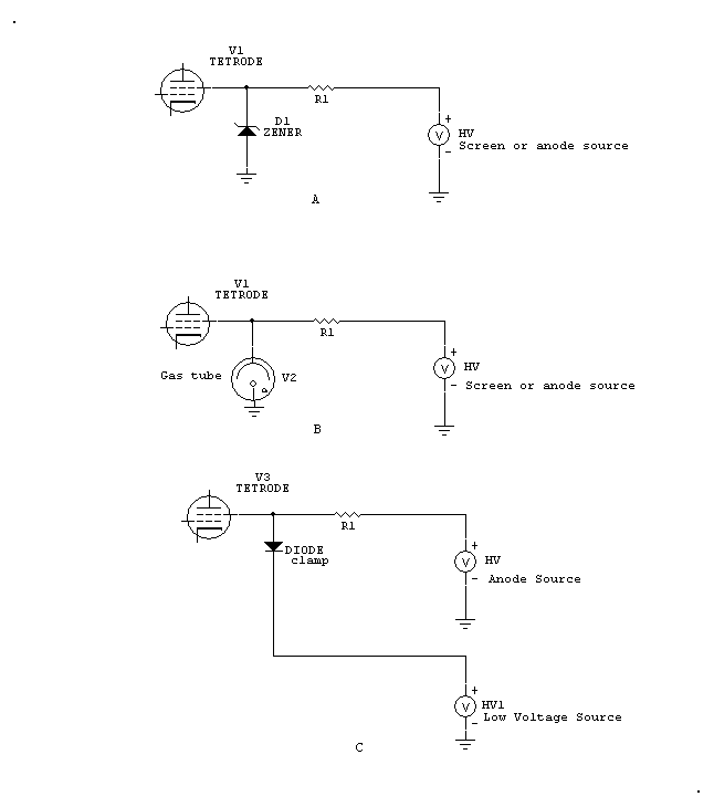
You'll notice the above circuits omit a standard voltage divider. This is because a standard voltage divider either limits dissipation to a safe value, or limits voltage to a safe value. Although better than just a standard single resistor dropping system, a voltage divider generally cannot do both!
A: Series resistance and shunt Zener.
This simple circuit uses a Zener diode for regulation.
B: Series resistance and shunt gas tube
This circuit uses a shunt gas tube, and has all of the problems associated with gas regulator tubes. Gas regulator tubes require more ignition voltage than sustaining voltage. Refer to the VR Tube design section at this link where you can download a Spreadsheet
C: Clamping Diode to LV
Boat anchor affectiono should pay attention to this method. This circuit uses a clamping diode divert current in key-up or light screen load conditions to a bleeder loaded low voltage supply. The low voltage supply must be reasonably stable, and the LV supply must be able to accept and safely absorb current from the screen dropping resistor without seriously affecting the low voltage supply stability. This screen supply method is often acceptable in minimal-cost class C tube type transmitter designs, as long as the LV supply has an adequate bleeder resistance. For just a few cents in parts, this circuit can correct screen key-up soaring in CW transmitters (which generally cause abnormal CW key voltages).
The circuits above, with proper HV and components, will satisfy all safety and operating requirements. They will provide a safe, reliable, simple, properly-operating screen supply at very little complexity or cost.
In all circuits, R1 should be set to limit current at the maximum desired screen current. Any shunt regulator, Zener or gas, should be at the desired screen voltage and properly rated for dissipation.
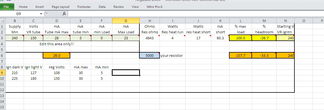
Here is a basic spread sheet download:
Basic Screen Grid Circuits
The screen grid can go into a negative resistance region, supplying current to the screen source instead of drawing current. In severe cases, this can cause the screen to go above supply rail. This can lead to excessive screen voltage.
As mean or average anode voltage sags nearer or below screen voltage, screen resistance drops and screen current soars. This can lead to excessive screen dissipation. Because of this, the screen also needs current limiting.
Shunt regulators operated from a high source voltage mitigate the two factors above, negative resistance and low screen resistance.
There is an Excel sheet to calculate regulator dissipation and current on this page. The Excel link is Regulator Spreadsheet. This sheet will work with diodes or gas tubes.
Let's look at two possible shunt regulator choices:
A general rule of thumb is we set the dissipation in the regulator at the value of maximum allowed grid dissipation, and have a regulator with enough dissipation headroom to safely absorb any negative screen current. A conservative estimate would to use a regulator capable of dissipating twice the screen rated dissipation. Ideally, we also want to have HV supply voltage between 1.5 times and twice the operating screen voltage. The ration can be more than 2, but at the expense of screen resistor and regulator heat.